- 您现在的位置:买卖IC网 > Sheet目录314 > AT93C86AY6-10YH-1.8 (Atmel)IC EEPROM 16KBIT 2MHZ 8MAP
�� �
�
�AT93C86A�
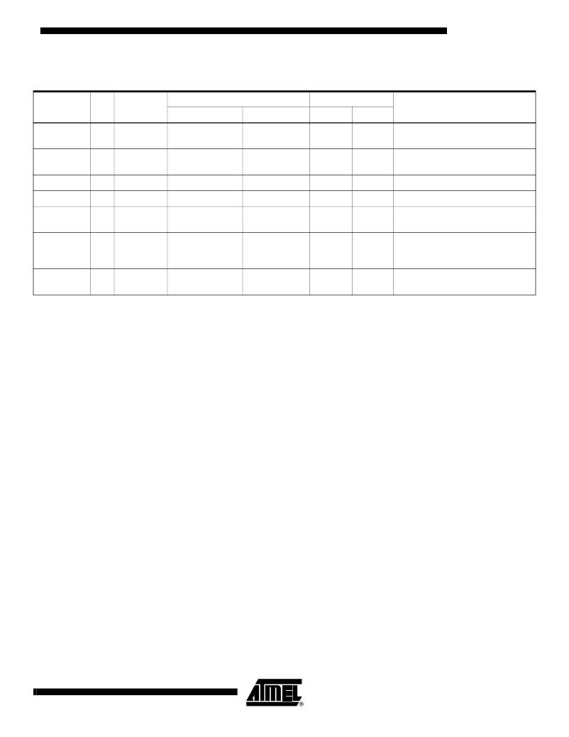
�Table� 5.� Instruction� Set� for� the� AT93C86A�
�Address�
�Data�
�Instruction�
�READ�
�EWEN�
�SB�
�1�
�1�
�Op� Code�
�10�
�00�
�x8�
�A� 10� –� A� 0�
�11XXXXXXXXX�
�x� 16�
�A� 9� –� A� 0�
�11XXXXXXXX�
�x8�
�x� 16�
�Comments�
�Reads� data� stored� in� memory,�
�at� specified� address.�
�Write� enable� must� precede� all�
�programming� modes.�
�ERASE�
�1�
�11�
�A� 10� –� A� 0�
�A� 9� –� A� 0�
�Erases� memory� location� A� n� –� A� 0� .�
�WRITE�
�ERAL�
�1�
�1�
�01�
�00�
�A� 10� –� A� 0�
�10XXXXXXXXX�
�A� 9� –� A� 0�
�10XXXXXXXX�
�D� 7� –� D� 0�
�D� 15� –� D� 0�
�Writes� memory� location� A� n� –� A� 0� .�
�Erases� all� memory� locations.�
�Valid� only� at� V� CC� =� 4.5V� to� 5.5V.�
�WRAL�
�EWDS�
�1�
�1�
�00�
�00�
�01XXXXXXXXX�
�00XXXXXXXXX�
�01XXXXXXXX�
�00XXXXXXXX�
�D� 7� –� D� 0�
�D� 15� –� D� 0�
�Writes� all� memory� locations.�
�Valid� when� V� CC� =� 4.5V� to� 5.5V� and�
�Disable� Register� cleared.�
�Disables� all� programming�
�instructions.�
�Functional�
�Description�
�The� AT93C86A� is� accessed� via� a� simple� and� versatile� three-wire� serial� communication�
�interface.� Device� operation� is� controlled� by� seven� instructions� issued� by� the� host� pro-�
�cessor.� A� valid� instruction� starts� with� a� rising� edge� of� CS� and� consists� of� a� Start� Bit�
�(logic� “1� ”)� followed� by� the� appropriate� Op� Code� and� the� desired� memory� address�
�location.�
�READ� (READ):� The� Read� (READ)� instruction� contains� the� address� code� for� the� mem-�
�ory� location� to� be� read.� After� the� instruction� and� address� are� decoded,� data� from� the�
�selected� memory� location� is� available� at� the� serial� output� pin� DO.� Output� data� changes�
�are� synchronized� with� the� rising� edges� of� serial� clock� SK.� It� should� be� noted� that� a�
�dummy� bit� (logic� “0”)� precedes� the� 8-� or� 16-bit� data� output� string.� The� AT93C86A� sup-�
�ports� sequential� read� operations.� The� device� will� automatically� increment� the� internal�
�address� pointer� and� clock� out� the� next� memory� location� as� long� as� CS� is� held� high.� In�
�this� case,� the� dummy� bit� (logic� “0”)� will� not� be� clocked� out� between� memory� locations,�
�thus� allowing� for� a� continuous� stream� of� data� to� be� read.�
�ERASE/WRITE� (EWEN):� To� assure� data� integrity,� the� part� automatically� goes� into� the�
�Erase/Write� Disable� (EWDS)� state� when� power� is� first� applied.� An� Erase/Write� Enable�
�(EWEN)� instruction� must� be� executed� first� before� any� programming� instructions� can� be�
�carried� out.� Please� note� that� once� in� the� EWEN� state,� programming� remains� enabled�
�until� an� EWDS� instruction� is� executed� or� V� CC� power� is� removed� from� the� part.�
�ERASE� (ERASE):� The� Erase� (ERASE)� instruction� programs� all� bits� in� the� specified�
�memory� location� to� the� logical� “1”� state.� The� self-timed� erase� cycle� starts� once� the�
�ERASE� instruction� and� address� are� decoded.� The� DO� pin� outputs� the� Ready/Busy� sta-�
�tus� of� the� part� if� CS� is� brought� high� after� being� kept� low� for� a� minimum� of� 250� ns� (t� CS� ).� A�
�logic� “1”� at� pin� DO� indicates� that� the� selected� memory� location� has� been� erased,� and� the�
�part� is� ready� for� another� instruction.�
�WRITE� (WRITE):� The� Write� (WRITE)� instruction� contains� the� 8� or� 16� bits� of� data� to� be�
�written� into� the� specified� memory� location.� The� self-timed� programming� cycle� t� WP� starts�
�after� the� last� bit� of� data� is� received� at� serial� data� input� pin� DI.� The� DO� pin� outputs� the�
�Ready/Busy� status� of� the� part� if� CS� is� brought� high� after� being� kept� low� for� a� minimum� of�
�5�
�3408H–SEEPR–1/07�
�发布紧急采购,3分钟左右您将得到回复。
相关PDF资料
ATAVRBFLY
KIT EVALUATION AVR BUTTERFLY
ATAVRXBNDL
XMEGA XPLAIN AND DISPLAY MODULE
ATDH2222
ADAPTER FOR ATDH2200 20PLCC
ATDH2225
CABLE ISP FOR AT17
ATDH2227
ADAPTER FOR ATDH2200 44PLCC
ATEVK1101
KIT DEV/EVAL FOR AVR32 AT32UC3B
ATF15XXDK3-SAX20
KIT DEV 20TSSOP ADAPTER ATF15XX
ATJTAGICE2
AVR ON-CHIP D-BUG SYSTEM
相关代理商/技术参数
AT93C86AY6-10YH-1.8 SL383
制造商:Atmel Corporation 功能描述:EEPROM Serial-3Wire 16K-Bit 2K x 8/1K x 16 2.5V/3.3V/5V 8-Pin UDFN EP T/R 制造商:Atmel Corporation 功能描述:SERIAL EEPROM, 16K (2K X 8 OR 1K X 16), 3-WIRE - 8 UDFN, PB/ - Tape and Reel
AT93C86AY6-10YH-1.8-T
功能描述:IC EEPROM 16KBIT 2MHZ 8MLP 制造商:microchip technology 系列:- 包装:剪切带(CT) 零件状态:Digi-Key 停止供應 存储器类型:非易失 存储器格式:EEPROM 技术:EEPROM 存储容量:16Kb (2K x 8,1K x 16) 时钟频率:2MHz 写周期时间 - 字,页:10ms 存储器接口:SPI 电压 - 电源:1.8 V ~ 5.5 V 工作温度:-40°C ~ 85°C(TA) 安装类型:表面贴装 封装/外壳:8-UFDFN 裸露焊盘 供应商器件封装:8-Mini Map(2x3) 基本零件编号:AT93C86 标准包装:1
AT9410
功能描述:开关配件 RND SPLSH COV LB RoHS:否 制造商:C&K Components 类型:Cap 用于:Pushbutton Switches 设计目的:
AT945
制造商:ATMEL 制造商全称:ATMEL Corporation 功能描述:Secure 5K - 40K Gates of AT40K FPGA with 8-bit Microcontroller,up to 36 Kbytes of SRAM and On-chip Program Storage EEPROM
AT94K
制造商:ATMEL 制造商全称:ATMEL Corporation 功能描述:5K - 40K Gates of AT40K FPGA with 8-bit Microcontroller, up to 36K Bytes of SRAM and On-chip JTAG ICE
AT94K05
制造商:ATMEL 制造商全称:ATMEL Corporation 功能描述:5K - 40K Gates of AT40K FPGA with 8-bit Microcontroller, up to 36K Bytes of SRAM and On-chip JTAG ICE
AT94K05AL-25AJC
功能描述:FPGA - 现场可编程门阵列 144 PROD PKG - 84 RoHS:否 制造商:Altera Corporation 系列:Cyclone V E 栅极数量: 逻辑块数量:943 内嵌式块RAM - EBR:1956 kbit 输入/输出端数量:128 最大工作频率:800 MHz 工作电源电压:1.1 V 最大工作温度:+ 70 C 安装风格:SMD/SMT 封装 / 箱体:FBGA-256
AT94K05AL-25AJI
功能描述:FPGA - 现场可编程门阵列 FPGA COM TEMP PROD PKG IND TEMP RoHS:否 制造商:Altera Corporation 系列:Cyclone V E 栅极数量: 逻辑块数量:943 内嵌式块RAM - EBR:1956 kbit 输入/输出端数量:128 最大工作频率:800 MHz 工作电源电压:1.1 V 最大工作温度:+ 70 C 安装风格:SMD/SMT 封装 / 箱体:FBGA-256